
San Francisco · Est. 2011
Solving complex technology problems through rigorous materials science.
Solar cell architecture, wet-clean chemistry and 3D GPU–CPU semiconductor packaging design — engineered with precision. Made in USA.
Mission
From terrestrial grids to space platforms, advancing materials science and process engineering to overcome complex technical barriers — delivering measurable and significant gains in performance, purity, reliability and degradation resistance.
Partner with us to advance the next generation of high-performance technology. Start a conversation →
Focus areas
Three problems we work on.
01 Bifacial Solar Cell9 issued patents · TOPCon patent pending
Bifacial Solar Cell Architecture
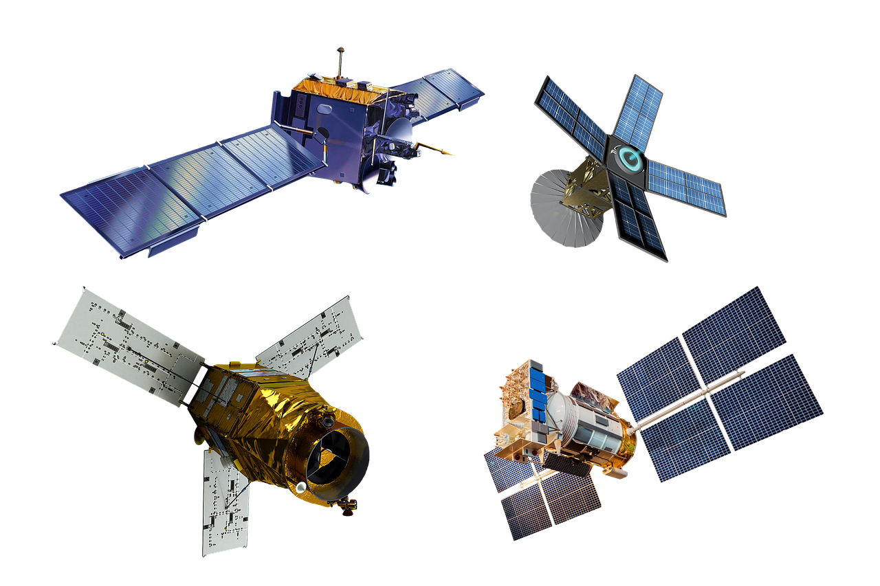
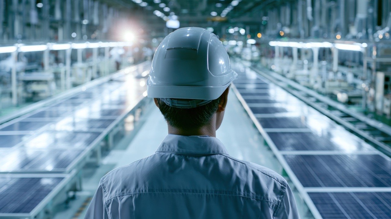
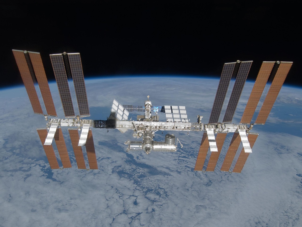
Nine issued patents covering bifacial solar panel technology and cell architecture — capturing energy from both faces of a panel, with reflectors returning light to the rear. Our R&D targets grid-connected terrestrial markets and the more demanding reliability and performance requirements of space-qualified photovoltaics.
TOPCon P-Type Contact Layer
A novel contact-layer innovation for Tunnel Oxide Passivated Contact cells, developed through chemical-engineering work in material synthesis, surface passivation and process chemistry — to improve yield and bifacial cell efficiency.
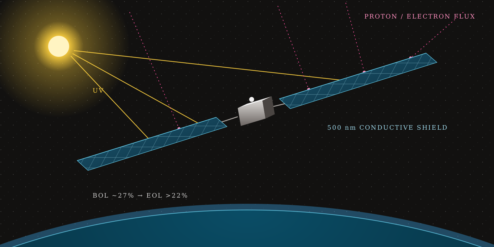
This design solves solar cell degradation in space.
- 01Vertical current collection replaces lateral collection in the p-type contact of standard n-type TOPCon cells, reducing recombination losses.
- 02Modified band structure adds electron/hole separation and collection pathways, so carriers are extracted faster even with radiation-induced defects.
- 03Thinned cell — compatible with existing terrestrial TOPCon lines via one added thinning step — shortens carrier travel and strengthens the internal field.
- 04~27% starting efficiency means that even after 20% radiation degradation, efficiency stays above 22%.
- 05500 nm conductive front-surface layer dissipates charge and shields against UV.
02 Particle CleaningChemical production facility
Chemical Engineering of Wet Cleaning Solutions
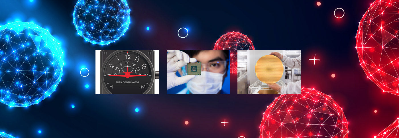
Wet cleaning solutions for contamination-sensitive, high-precision parts manufacturing and specialty industrial applications — made in our own chemical production facility for semiconductor, aerospace and PV customers.
03 3D GPU–CPU PackagingIn development
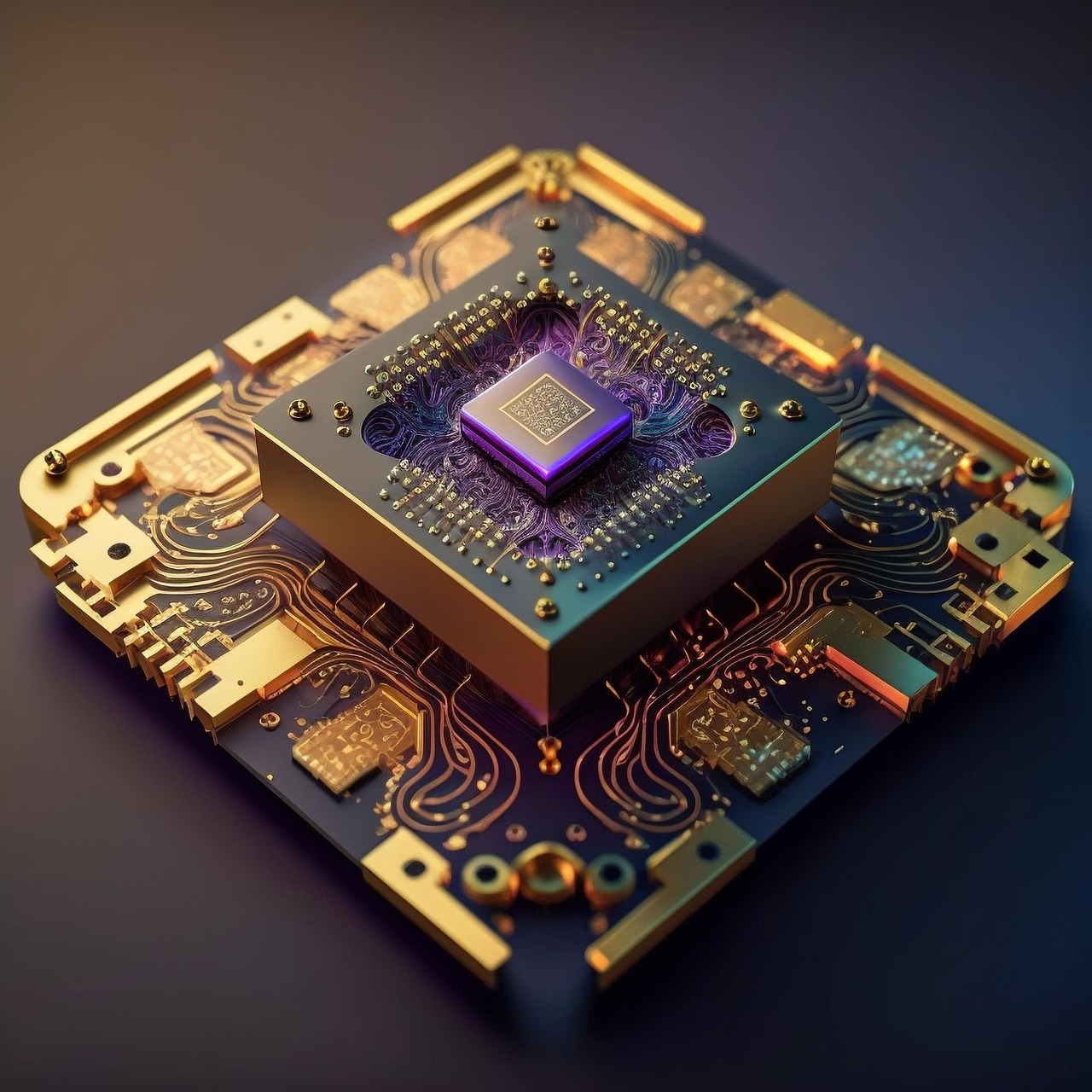
Novel 3D GPU–CPU Semiconductor Packaging Design
A new approach to compute-stack architecture aimed at solving some of the most pressing problems facing the industry — vertical interconnect density, bandwidth and heat.
BWstack = Nvia · fvia · b
Current initiative · DOE SPACEPV / PARSECS
Taking the TOPCon p-type contact layer from patent-pending to manufacturing scale.
Bakersun is pursuing DOE SPACEPV / PARSECS research funding, with founder Ivan Scheulov as prime investigator.
Leadership
Ivan Scheulov
Founder, CEO & CMO
Inventor of record on Bakersun’s bifacial solar cell patents and principal investigator on its TOPCon p-type contact layer R&D. Twenty-plus years of product engineering and program management leadership at technology and solar PV start-ups, the California Academy of Sciences, and one of the top energy utilities in the USA, Florida Power & Light.
Advisory team
Ivan works alongside a consulting team of expert advisors and mentors, including PhD-level chemical and electrical engineers, backed by a network of laboratory and testing facilities that support development from material synthesis through validation.
Origin
What’s in the name — BakerSunTech?
The ideas took shape on the shore of Baker Beach in San Francisco — a place for solo recharge and brainstorming, between the elements and an engineering marvel: the Golden Gate Bridge. At the time, the intense work of building and growing a solar PV start-up was driving research into the optimum solar cell architecture, and into a manufacturing process for a novel TOPCon stack.
Under brief sunlight breaking through the coastal fog, the first solutions were sketched. The sketches moved to the whiteboard, the whiteboard became a mathematical model, and the model became patented technology — and, in turn, new ideas. Since the early 2000s, this spot has been a source of motivation to solve interesting problems. Hence the name: Baker for the beach name and its heat and elements exposure, Sun for the source of energy, Tech for what follows.
Bring us a pressing problem.
Licensing, research partnerships, or cleaning chemistry for your line.